Hot Chips 32, XSX Architecture Deep Dive

I know this article but even here in the quote from Eurogamer article, you can clearly read it is speculation on their part “It is reasonable to assume that (…) somehow” It is not a confirmation from their part at all. The terms they use are highly speculative, reasonable assumptions not confirmations.

And it shows they didn’t probably see the video conference but only the powerpoint cause it was not available at the moment, otherwise they would have mentionned the L3 question thing with Jeffrey Andrews cause it logically raises eyebrows.

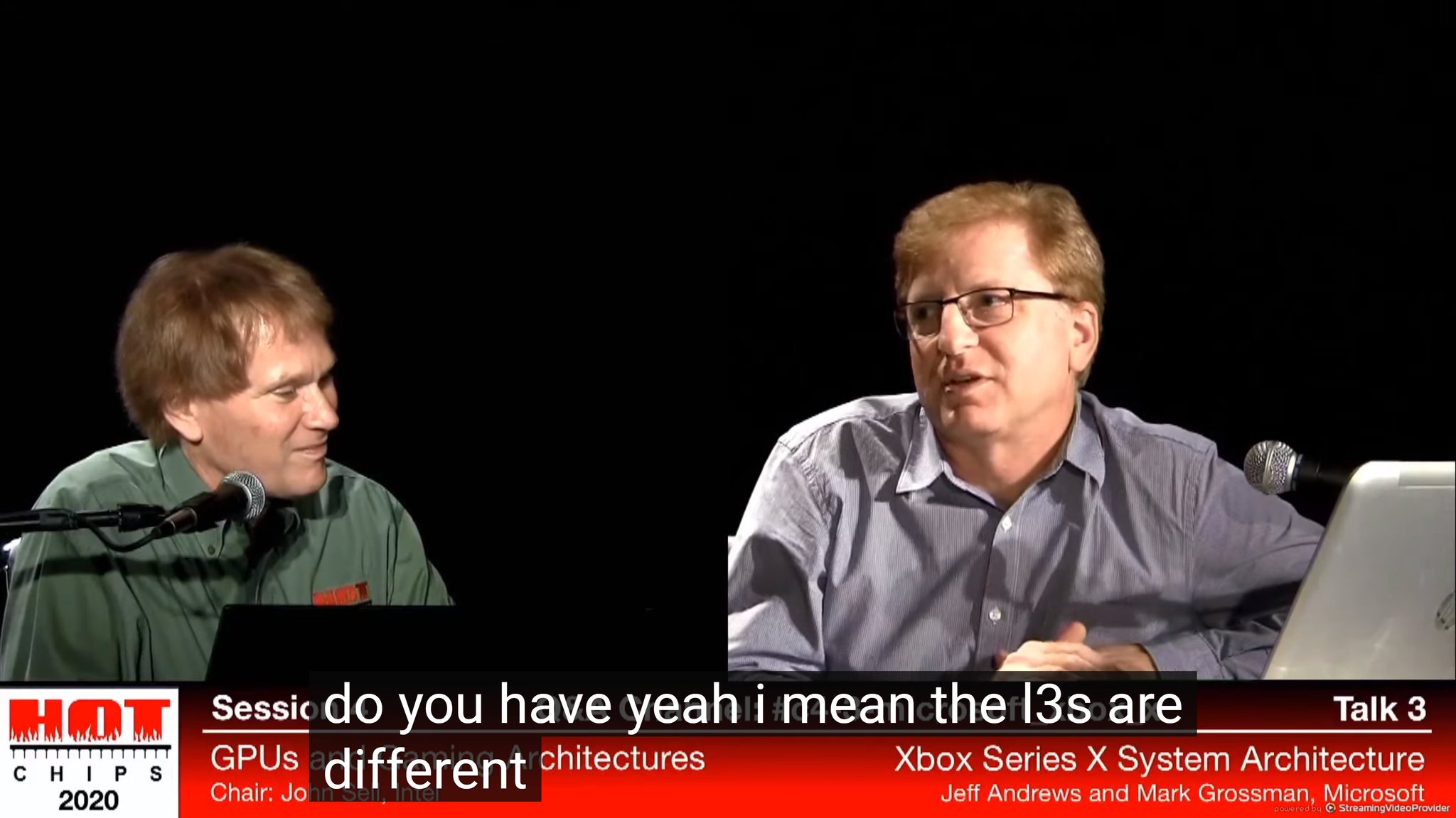
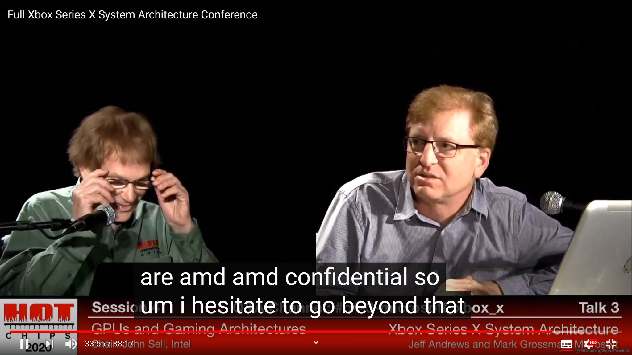
Also you heard it clearly in the video I posted with the exact timestamps at 33:30 when Jeffrey Andrews CPU architect spoke about AMD NDA about the cache, I’m not fabricating it.

Here the timing and chronology is really important to have a better understanding.

The HotChips video conference is from a date way anterior to the RDNA2 conference. That is why they had to wait for AMD to reveal RDNA2. The RDNA2 officialisation was on the 28th of october. Maybe they now can talk about it. Maybe…

MS clearly said all the RDNA2 features showed (including Infinity Cache feature) by AMD were hardware supported by Xbox Series X/S

Infinity Cache is an RDNA2 feature, Xbox Series X/S are the ONLY next gen consoles with FULL RDNA2. Meaning XSX has Infinity Cache…It is clear. I already brought the official source above posts earlier. “Xbox Series X|S are the only next-generation consoles with full hardware support for all the RDNA 2 capabilities AMD showcased today.”

AMD showcased Infinity Cache this day as a RDNA2 feature…So voilà. :wink:

Btw for the 128MB where did AMD said it was mandatory to have 128MB? Which is why it’s the same size across all RX 6000 GPU revealed so far. But who says the size needed to be the same?

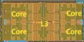
L3s of the SX CPU is 4MB per CCX compared to 16MB on desktop Zen 2. Right? Meaning that’s 1/4th the size.

So why couldn’t the XSX have an Infinity Cache 1/4th the size of what AMD is putting in desktop RX 6000 GPUs also? So 32MB infinity cache.

Nobody answered my questions before in my precedent post about MS using the same strategy :sweat_smile: why would they change strategy then now? Seems to have the same function as below:

“On-chip caches for GPU usage are not a new idea, especially for AMD. The company included a 32MB eSRAM cache for the Xbox One (and Xbox One S) SoC, and even before that the Xbox 360 had an on-package eDRAM as well. But this is the first time we’ve seen a large cache on a PC GPU.”

The infinity cache seems like an updated version of what MS did previously on X360 and Xbox One with eDram & eSram. That’s why it might be really useful for full efficiency on the XSX like I quoted above “allowing the GPU to more quickly fetch data rather than having to wait around for it to come in from VRAM” for example.

The infinity cache plays the role as a massive bandwith amplificator.

Microsoft consoles have provided the biggest hardware and software gaming technologies to the industry, which Microsoft has always shared with and used to advance Windows (DirectX) and PC hardware needs. They continue doing it with bringing new tech to PC world so I’m not surprised.

Maybe someone can ask Jason Ronald or Jeffrey Andrews or Lisa Su about the Infinity Cache and its relation with XSX.

Because Ms told them only the total cache, not the full configuration. The information is that SX had 76MB total of cache, the speculation is that this means that compared to PC the cpu would have reduced L3 size (and that was correct, the sx cpu have only 8mb of L3 cache compared to an enormous 32MB on the desktop version).

He said sx had a server-class cpu, he was asked why it is server class when it’s missing the 32MB of cache from the desktop cpus.

His answer was: The caches are not exactly the same, because AMD made optimizations that I can’t disclose.

You are implying this means they have some hidden soc details, but they disclosed the whole thing. Everyone coding for this will know exactly what it has/hasn’t. His unwillingness to share implementation details on how that affects performance is not relevant.

Because even only 32MB of infinite cache would be bigger than the entire CPU block (counting even the 8MB L3 cache), does that really seem reasonable to you?

Look at how big even 4MB of sram is:

image

Literally 1/3 of each cpu is just 4MB of cache.

Again, it’s just not reasonable, even 32MB of cache would make the rest of the soc area smaller than what you have on PS5.

That strategy got us the xbone. That literally replaced processing area for cache and was a disaster for them.

They already moved past that on the X, and SX just continues on that approach.

It’s just not reasonable for a console, where every mm2 matters. In fact, if you watch the hotchips presentation they touch on that exact point almost all the time.

They had to be super conscious about die area because they are hitting a limit on what’s viable to put into an SoC.

It does, but they also touch on the subject during hot chips.

On xbone they used a cache to reduce memory costs. Didn’t work.

On X they went the exact other direction: Went with the most expensive memory solution they could afford so bandwidth wasn’t a problem.

That approach is no longer viable, so for SX they had to mix it up:

  • They increased cache amount and their efficiencies (SX gpu has 5MB of L2 cache, compared to 4MB on 6800)
  • Better compression/texture formations on the GPU side
  • The split memory setup was a way to increase the bandwidth without increasing the costs that much.
  • Even then it wasn’t enough for their performance targets, so they had to come up with hardware features such as VRS

They also talked about how an HBM setup could have solved their BW issues, but there’s the drawback that HBM does not deal as well with multiple consumers as gddr does (so it would be a bottleneck with the cpu, audio, and ssd fighting for bandwidth at the same time)

4 Likes

For some strange reason youtube recommended me a new video about PS 5 having RDNA 3. Are people this crazy?

The #1 thing that I find fascinating about next gen hardware is it’s capabilities in terms of ML. Maybe that’s more of a tools topic…but I don’t think it entirely is. Combining ML and cloud compute could bring some paradigm shifts to game design and game development IMO. Anyone have good links or resources on this topic.

5 Likes

@LucasTaves thx for the detailed response so I don’t had to do it.

1 Like

Much like everything involving ML it’s straight up magic in several gaming design areas.

Basically using ML to train the game how super complex simulations should work is orders of magnitude faster than actually simulating them.

Even with super complex soft body simulations, deformation, fluids, smoke, etc.

I can’t imagine how insane is going to be the evolution when ML is in full swing on game creation. Because it can potentially enhance all areas from content production, graphics quality, performance, physics, animation, IA…

5 Likes

That was one of the videos I was going to post myself, it’s a great one and I can find some others if anyone needs additional resources. Coupled with things like OpenAI, I firmly believe that ML hardware on the Series S/X and Nvidia/AMD will be the most impactful innovation this generation, as it can fundamentally enhance the developer and user experience in nearly limitless ways. For example, ML can be used to provide NPCs with special awareness and player-impact awareness; imagine an RPG where an NPC reacts to everything that happens in the world beyond just a few canned animations or responses.

This generation of consoles will bring some of the biggest leaps seen, but I think Microsoft’s holistic, forward-thinking approach will pay in dividends as the generation goes on. RDNA2 (VRS, Mesh shaders, especially), DX12U, ML hardware, superior audio block, and all the other custom solutions (both hardware and software) will enable greater innovation and technical leaps than an SSD alone ever could.

2 Likes

Another example!

It’s not in run time but still impressive.

3 Likes

Here’s another from Unity Labs:

3 Likes

Awesome stuff! Thank you!

3 Likes

That’s awesome. I can only imagine how much work lip sincing multiple languages is, since no one does it.

1 Like

Hey! Glad to see a good answer and perspective. I really appreciate your point of view even if our views differ.

But I have to disagree with you. Why MS announced a total cache of 76MB to only have 12MB in the end. Such a drastic change. How can they not be aware of that in advance and made last minute change then still call it server class… Maybe they have another configuration for Azure use.

XSX Apu dimensions based on hotchips 2020

GPU : 170 mm² CPU : 36 mm² GGDR6 controllers + IO : 94 mm² Audio controller + multimedia : 20 mm² SOC fabric : 40 mm²

Total : 360 mm² it fits correctly

If we look closer the CPU cache is around 8 mm². So 2 mm² for 1 mo.

If we calculate we arrive logically at 128mm² to add the 64 mo cache.

So it is 1/3 the dimension of the APU located elsewhere than on the die shot from Hotchips 2020.

5Mo cache L2 for the GPU + 4Mo de Cache for the CPU (8x512ko). 9Mo + eventually 3Mo for L0 & L1 GPU caches. So a total of 12Mo. Where are the missing 64? Why such a disparity?

How is it possible to miscalculate at this point to go from a huge 76MB cache classified as server class to 12MB equal as a mobile class. Why is it still called server class then? Something is not right. What is the logical explanation for that?

Sorry but It is not optimization but reduction at this point with such a large gap and you are misquoting Jeffrey Andrews by saying what he didn’t by saying AMD made optimizations. Which optimizations you think of? Also he clearly said what I quoted he didn’t say optimization but I understood that’s what you understood. He said also they would talk of key innovations in the time they have (meaning they didn’t probably have time for everything).

What do you make of the official quote from MS then saying “Xbox Series X|S are the only next-generation consoles with full hardware support for all the RDNA 2 capabilities AMD showcased today.”

Do you discard it?

Infinity Cache is a RDNA2 feature also and MS said the above so what do you make of that.

Infinity cache is a fancy name like I said is also used a bandwith multiplier and it looks like to share the same function as Xbox Velocity Architecture go watch both and compare.

“With this insight, we were able to create and add new capabilities to the Xbox Series X GPU which enables it to only load the sub portions of a mip level into memory, on demand, just in time for when the GPU requires the data. This innovation results in approximately 2.5x the effective I/O throughput and memory usage above and beyond the raw hardware capabilities on average. SFS provides an effective multiplier on available system memory and I/O bandwidth, resulting in significantly more memory and I/O throughput available to make your game richer and more immersive.”

I also think I think the virtual RAM on the XSX is implemented using an HBCC (High Bandwidth Cache Controller) combined with the SFS to make the data transfer with fine granularity way more efficient and more accurate.

What do you make also of the Direct ML hardware capabilities? How they can claim a component of DirectX DirectML leverages unprecedented hardware performance in a console. Benefiting from over 24 TFLOPS of 16-bit float performance, and over 97 TOPS (trillion operations per second) of 4-bit integer performance on Xbox Series X while on the die we don’t see Direct ML hardware accelerated cores or compute untis dedicated for that while showing features like auto HDR at a system level without needing the devs to participate and having no impact on available CPU, GPU or memory ressources? Where is it then?

Ms said clearly “Through close collaboration and partnership between Xbox and AMD, not only have we delivered on this promise, we have gone even further introducing additional next-generation innovation such as hardware accelerated Machine Learning capabilities for better NPC intelligence, more lifelike animation, and improved visual quality via techniques such as ML powered super resolution.”

RDNA2 doesn’t have Int4/Int8 so by saying this it means they added extra silicon for additional hardware capabilities for Machine Learning right but where is it on the die shot? I don’t see it. Look at it again please. For example, RDNA2 has only Sampler Feedback and MS add their own streaming tech to the Sampler Feedback and tell me.

Of course all is speculation from both of us. I already talked privately to engineers, coders, programmers and devs about that theory and they all said it could be possible like your theory is possible too. We both have our views but they are both valid in some ways. We can also be wrong on some others. In the end it is just a discussion. MS and AMD only know the truth behind. Feel free to add your thoughts. I appreciate the discussion and wait for your answer.

Are you not getting that mixed up with the “multiplier” Sampler Feedback provides?

Can you elaborate please?

You posted a quote about SF providing a multiplier after talking about IC.

You also claimed IC is an RDNA2 feature, it isn’t.

1 Like

What are you talking about? There is no change. The total is still 76mb. But that’s counting all total sram in the soc.

I really don’t get what you mean.

But just to state 2 separated facts:

  • Ms claimed SX has a total 76mb of cache in the soc.
  • Ms claimed that the cpu has server class performance, despite the reduction in L3 cache we see in the desktop size.

The reason for the second is that L3 cache is usually attributed to the performance gains from Ryzen 1 to 2. And against that point Ms made the claim that Amd made other optimizations so the performance doesn’t drop as you would expect from such a drastic cache drop. Those optimizations are not exclusive to SX I think, just regular architecture changes from Ryzen to Ryzen 2 I believe. Keep in mind that Ryzen 2 laptop cpus took the entire industry by surprise literally because no one believed they would be so good and didn’t have the hardware to use it.

No. But as the quote clearly states, they were talking about gpu capabilities that were brought on rdna2.

Infinite cache is not a new capability, it’s simply a different memory subsystem to increase the memory bandwidth. And it doesn’t even mean it’s the best choice. Case in point the xbone. Did the esram improved the performance over the paltry 68GB/s it had? Definitely. Did it matched or surpassed the sheer amount of bandwidth ps4 memory setup provided? No.

No. The fact that they both used the term effective multiplier and the quoted number of 2.5 is just a coincidence. They are completely different from each other and the meaning is so as well.

Infinite Cache works as a memory bandwidth multiplier because every single part of the gpu can access it and if the data is cached it will literally be faster than the external memory.

SFS works as a SSD bandwidth multiplier because it effectively reduces the amount of data you need to load. Same as an effective memory amount multiplier. If you only really need 30% of the textures you load a hardware that tells you don’t need the 70% effectively multiplied your ram amount and the SSD speed.

That’s completely explained by them. The CU is modified so the execution unit can take multiple integers at the same time. Without this feature it would only be able to execute a single operation even if the registers were idle. They also made a case that the increased die area over the CUs without this feature is almost irrelevant.

Gpus can process int numbers for a long time now. The difference is the throughput. The change is exclusively about how the CU can use the existing hardware to execute more numbers at the same time.

This is well documented by AMD’s architecture white paper: https://www.amd.com/system/files/documents/rdna-whitepaper.pdf

Specifically:

To accommodate the narrower wavefronts, the vector register file has been reorganized. Each vector general purpose register (vGPR) contains 32 lanes that are 32-bits wide, and a SIMD contains a total of 1,024 vGPRs – 4X the number of registers as in GCN. The registers typically hold single-precision (32-bit) floating-point (FP) data, but are also designed for efficiently RDNA Architecture | 13 handling mixed precision. For larger 64-bit (or double precision) FP data, adjacent registers are combined to hold a full wavefront of data. More importantly, the compute unit vector registers natively support packed data including two half-precision (16-bit) FP values, four 8-bit integers, or eight 4-bit integers.

Ms also detailed extensively how SFS is implemented. They modified the texture units (they also detailed which parts of it and why), which is why, like the ML inference acceleration, you won’t see separated blocks for it.

That’s not entirely true. Both of them publishes patents and white papers so while the exact implementations are obviously not shared you can get a good idea on to why and how.

For example that’s how everyone knew AMD was attaching the RT acceleration hardware to the texture units months before they announced rdna2 details.

1 Like

@nrXic

Yes mixed it up 2 things apart indeed sorry my bad you’re right but why you say IC is not a full RDNA2 feature? How would you qualify it?

@LucasTaves

Nvm for now, forget what I said in the 1st paragraph I need to check something and will wait to have a confirmation I will probably continue the discussion with you by pm if you want. We’ll discuss it later.

You made some really good points I admit but I’m still doubtfull on some including the Int4/8 ML capabilities of the rdna gpus. RX 6800 series don’t seem to have it.

What is this? Look at the specs also please. Tell me what you think

Ms said the Auto HDR by Direct ML has no impact from the gpu or the cpu or even memory ressources so it is not inside those. It means 0 imho.

How can you explain it? It is hardware accelerator product.

https://www.amd.com/en/products/professional-graphics/instinct-mi50

Think about it 97 tops = MI50 AMD Where do you put those 97 T.Ops?

The point is CU on RDNA1 or 2 can’t run T.Ops it is only on High End machine learning accelerator I believe.

It has indeed CU indeed but beside it runs FP32 so it has Deep Learning ops if I’m not mistaken.

I don’t mean that is what MS is using exactly just to give a general concept idea.

Fo info, how many tiles has the XSX SOC?

If I’m not mistaken the Xbox One has 768 tiles.

Of course I agree, there are patents you can always find online and draw some conclusions but you never get the whole picture, the real truth and prupose is only known by those involved but I get what you mean.

Wow impressive. Direct ML is really future tech. Really promising tech. Indeed the enhancements to games could be potentially massive and even more incredible. Thanks for the share!

I am no expert here but IC is just a last level cache. Coupling a memory system with graphics system is not the right thing to do while doing nomenclature.

Also graphics features are meant to compute and memory features are meant to store and transfer. That’s a basic difference.

You can say IC is a feature of RX 6000 series cards but you can’t say it’s a feature of RDNA2.

3 Likes

Just as a cache to offset other deficits, much like how the X1 had it’s eSRAM. We didn’t call it part of the GC architecture, for example.

1 Like