Ah sorry, why we are talking about the 6800 series in a XSX hotchips thread again? I think that is the root of my confusion …
The guy I originally quoted was speculating that 6800 lacks int instructions because their rates were not listed.
I mentioned that even if it lacks the rpm feature in the very least the 6800 would be able to provide 16tops for them, so I wouldn’t read much into the fact that they are not listed.
Correct me but didn’t the 5700xt with the base, gaming, and boost clocks showed that most of the time in games it was in gaming clocks. AMD used the new naming for the clocks for a range it can do and tests showed gaming is where the gpu spends its time in many AAA games. That would put the 6800 at about 14TFs using the gaming clock which is close to XSX. Would be fun once DF gets the chance to compare them. I expect very close performance with the XSX and 6800
It is true, under normal circumstances, the AMD GPUs operate around the game clocks. If you add water cooling they are able to achieve higher clocks near the boost clock.
Thanks! So a standard 6800 will be pretty close to XSX performance ie 12.155TF vs 14TF
Probably 20-30% better than the XSX. Again console optimization is always the best (most of the time)

Around 31:45 and later at 33:30 keep your ears well open and listen carefully:
Question: “Is the CPU 3.8 giga hertz clock an all the time clock or is that a turbo frequency?”
Answer: “That’s an all the time clock…There’s been a lot of work in our team to have low dynamic range variation depending on the workload, so there’s been a decent amount of work to ensure that. So game developers don’t have to deal with oh I’m running through a certain code path with this dynamic data and now I’m seeing lots of variation on my framerate, that’s difficult for game developers.”
Lol…
Then a bit later on
Question: “In your presentation you said the Zen 2 CPUs are server class but it seems like the cache sizes are more of a mobile class, do you have a…?”
Answer: “Yeah I mean the L3s are different, I can’t, the problem is I can’t say too much cause I might say things that are AMD confidential so I hesitate to go beyond that…”
For those saying there is no Infinity Cache. There’s clearly an AMD NDA on the XSX L3 cache…
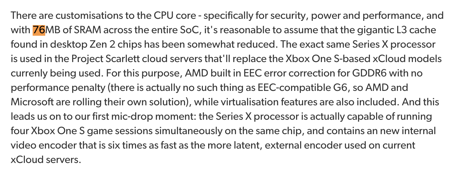
Plus DF spoke about 76MB cache back in march…They didn’t have access to the video conference since they talk only based on the powerpoint.
The plot thickens…
I can understand the AMD NDA. But won’t it be lifted by now?
Let’s wait 12 Nov to settle things on both the consoles.
The L3 cpu cache would have no relation to Infinite cache on the gpu.
We have the die shot, there’s nothing uncounted for in there. Look at the 6800 die shot, the infinity cache portion is significantly bigger than the entire SX cpu block, even at a fraction (say 32MB) you’d be looking for something at least around the whole cpu block.
That’s just not viable for consoles atm, the last time they decided to dedicate a significant die area for cache we had the xbone, again even 32MB of IC would make the logic area of the die smaller than the ps5 soc, so we would have another repeat of that design no one liked XD
2 Likes
Like Xbox one had second layer of GPU type secrets?
Lol
Oh stop it please. There is no hidden silicon.
2 Likes
The idea of whole hidden silicon is insane. Just imagine the implications, devs are making games using those hidden silicon. How can they keep NDA for this long for a product which is actually been shipped to consumers?
Any type of NDA beyond the release date of the product is simply flawed.
Please stop with that I’ve never said such a thing. Don’t put words into my mouth. Beware.
I showed you the proof that they couldn’t talk about everything inside, you heard it clearly in the video from Jeff Andrews the CPU Architect, he said the L3s are different and can’t speak about it cause there AMD confidential. It’s not me who said this it’s him. Ask him or AMD.
Why it is classified as server class then? Did you forget they will use also XSX for Azure?
What’s your argument against all of that then? Why there’s a confidentialilty on this part then, please explain.
Why flagging my post above? Am I forbidden to speak my mind or speculate? Or you pleased if I edited it and say “speculation”
Also why the idea of a nda beyond the release date of product is flawed? Why it is impossible? Remember when Jeff Andrews spoke about the AMD confidentiality the HotChips video conference is anterior to AMD RDNA2 conference. Maybe now the embargo is lifted since then.
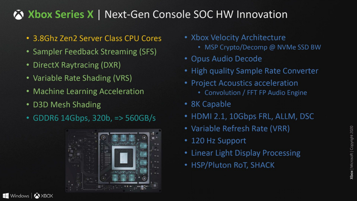
Why MS gone further and added “introducing additional next-generation innovation such as hardware accelerated Machine Learning capabilities.” The RX6000 series even on RDNA2 clearly don’t have it, just check.
MS clearly said “Xbox Series X|S are the only next-generation consoles with full hardware support for all the RDNA 2 capabilities AMD showcased today.”
“In our quest to put gamers and developers first we chose to wait for the most advanced technology from our partners at AMD before finalizing our architecture.”
Why MS would have an infinity cache what are the benefits?
MS is no stranger to that, why won’t they reiterate the same strategy?
“On-chip caches for GPU usage are not a new idea, especially for AMD. The company included a 32MB eSRAM cache for the Xbox One (and Xbox One S) SoC, and even before that the Xbox 360 had an on-package eDRAM as well. But this is the first time we’ve seen a large cache on a PC GPU.”
"There are several major advantages to having a large, on-chip cache, even in a GPU. As far as perf-per-watt goes, the cache further improves RDNA2’s energy efficiency by reducing the amount of traffic that has to go to energy-expensive VRAM. It also allows AMD to get away with a smaller memory subsystem with fewer DRAM chips and fewer memory controllers, reducing the power consumed there. Along these lines, AMD justifies the use of the cache in part by comparing the power costs of the cache versus a 384-bit memory bus configuration. Here a 256-bit bus with an Infinity Cache only consumes 90% of the power of a 384-bit solution, all the while delivering more than twice the peak bandwidth.
Furthermore, according to AMD the cache improves the amount of real-world work achieved per clock cycle on the GPU, presumably by allowing the GPU to more quickly fetch data rather than having to wait around for it to come in from VRAM. And finally, the Infinity Cache is also a big factor in AMD’s ray tracing accelerator cores, which keep parts of their significant BVH scene data in the cache"
Don’t get mad. I was just kidding.
But having secrets they will never tell doesn’t hold much weight.
Also, you don’t have to threaten me by using words like ‘beware’.
We can discuss arguments without getting aggresive.
2 Likes
I was not agressive or threatening you but I don’t like being clowned and mocked with your dual gpu reference that I have nothing to do with. We can discuss of course with respect. Sorry if you felt something like this from my part then. It was not my intent at all.
1 Like
Of course the L3 Cache is different in the Series APU than in Ryzen or RNDA2 graphics card. Because it is an APU with a shared memory setup. So CPU or GPU can see their stuff without the PCI express bus.
There is no infinity cache inside the Series X APU.
Understood. Lets shake hands and discuss next gen with mutual understanding ![]()
1 Like
Deal! I agree. Peace!
1 Like
MS was very open about their total cache size from the beginning starting with the Eurogamer article.
If you add up the standard caches that come with Zen2 and RDNA2 architectures you almost reach that number given (68MB). MS may changed some of the CPU L3 (which is 32MB) to a global L3 but that is it.
(the reason I did not understand the stance MS hiding something about their caches)
2 Likes
I’m so glad people are talking about cache. Anyone that has done engine optimization knows that for an engine to run smoothly you need to grab data off the cache. If you are grabbing data from RAM that will slow your game down. There are programmers that spend their entire day optimizing data so it’s available in cache and you don’t have to go out into RAM to get it. That’s why I laugh at all the SSD talk. High frame rate is achieved with cache optimization. Remember system RAM is considered too slow. SSD has no part in sustained frame rate.
3 Likes